Product Summary
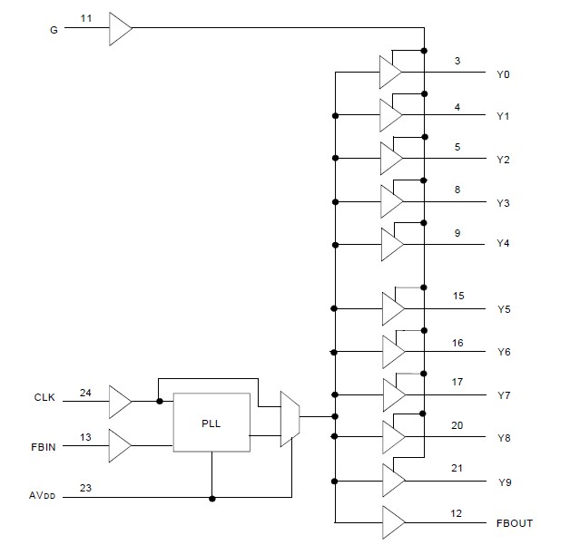
The CSP2510CPG is a high performance, low-skew, low-jitter, phase-lock loop (PLL) clock driver. It uses a PLL to precisely align, in both frequency and phase, the feedback (FBOUT) output to the clock (CLK) input signal. The CSP2510CPG is specifically designed for use with synchronous DRAMs. The device operates at 3.3V. One bank of ten outputs provide low-skew, low-jitter copies of CLK. Output signal duty cycles are adjusted to 50 percent, independent of the duty cycle at CLK. The applications of the CSP2510CPG include: SDRAM Modules, PC Motherboards, Workstations.
Parametrics
CSP2510CPG absolute maximum ratings: (1)VDD Supply Voltage Range: –0.5 to +4.6 V; (2)VI Input Voltage Range: –0.5 to +6.5 V; (3)VO Voltage range applied to any output in the high or low state: –0.5 to VDD + 0.5 V; (4)IIK (VI <0) Input clamp current: –50 mA; (5)IOK (VO <0 or VO > VDD) Terminal Voltage with Respect to GND (inputs VIH 2.5, VIL 2.5): ±50 mA; (6)IO (VO = 0 to VDD) Continuous Output Current: ±50 mA; (7)VDD or GND Continuous Current: ±100 mA; (8)TSTG Storage Temperature Range: – 65 to +150 ℃; (9)TJ Junction Temperature: +150 ℃.
Features
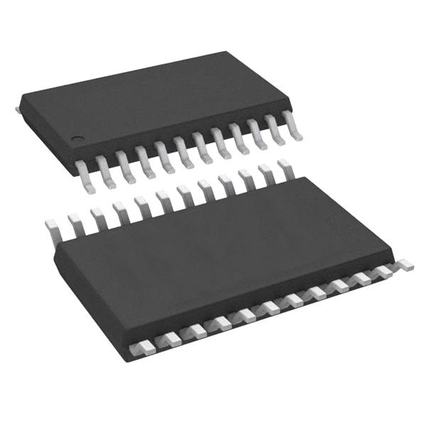
CSP2510CPG features: (1)Phase-Lock Loop Clock Distribution for Synchronous DRAM Applications; (2)Distributes one clock input to one bank of ten outputs; (3)Output enable bank control; (4)External feedback (FBIN) pin is used to synchronize the outputs to the clock input signal; (5)No external RC network required for PLL loop stability; (6)Operates at 3.3V VDD; (7)tpd Phase Error at 133MHz: < ±150ps; (8)Jitter (peak-to-peak) at 133MHz: < ±75ps @ 133MHz; (9)Spread Spectrum Compatible; (10)Operating frequency 25MHz to 140MHz; (11)Available in 24-Pin TSSOP package.
Diagrams

| Image | Part No | Mfg | Description |  |
Pricing (USD) |
Quantity | ||||||||||||
|---|---|---|---|---|---|---|---|---|---|---|---|---|---|---|---|---|---|---|
 |
 CSP2510CPG |
 Other |
 |
 Data Sheet |
 Negotiable |
|
||||||||||||
 |
 CSP2510CPG8 |
 Other |
 |
 Data Sheet |
 Negotiable |
|
||||||||||||
 |
 CSP2510CPGG |
 IDT |
 Clock Drivers & Distribution 10+1 Outputs PLL/Clk Driver |
 Data Sheet |

|
|
||||||||||||
 |
 CSP2510CPGG8 |
 Other |
 |
 Data Sheet |
 Negotiable |
|
||||||||||||
 |
 CSP2510CPGI |
 Other |
 |
 Data Sheet |
 Negotiable |
|
||||||||||||
 |
 CSP2510CPGI8 |
 Other |
 |
 Data Sheet |
 Negotiable |
|
||||||||||||
 (China (Mainland))


